Define the connections
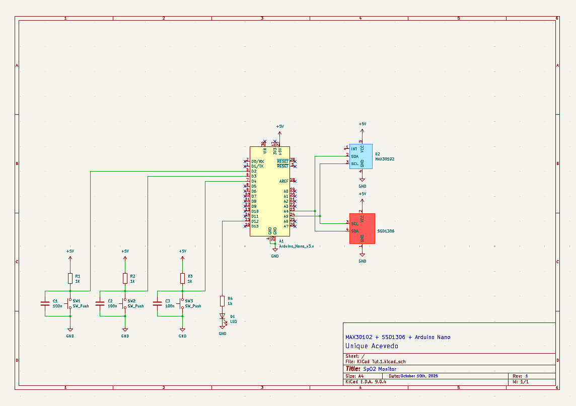
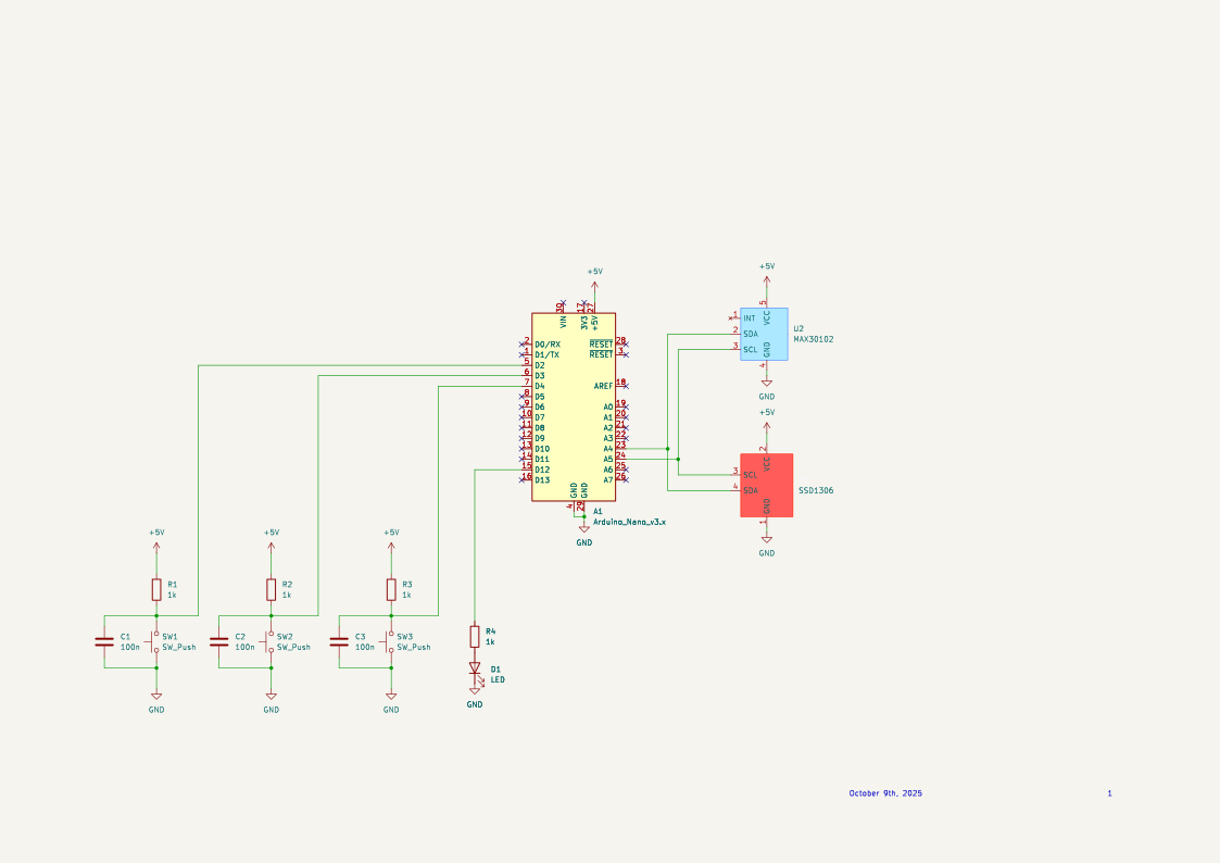
The Nano connects the optical sensor module and OLED display over I²C. The schematic also includes three push buttons, an indicator LED, and supporting resistors and capacitors.
Entry 02 / PCB design
From a system idea to a routed board.
Schematic & PCB layout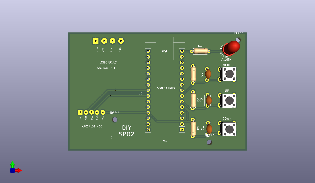 CAD RENDER
01 / The work
This project gave me practice turning a small sensing system into a complete KiCad design. I created the schematic, assigned footprints, routed the board, and exported the fabrication files. The work here is a PCB design; assembly, firmware integration, and measurements are still ahead.
The Nano connects the optical sensor module and OLED display over I²C. The schematic also includes three push buttons, an indicator LED, and supporting resistors and capacitors.
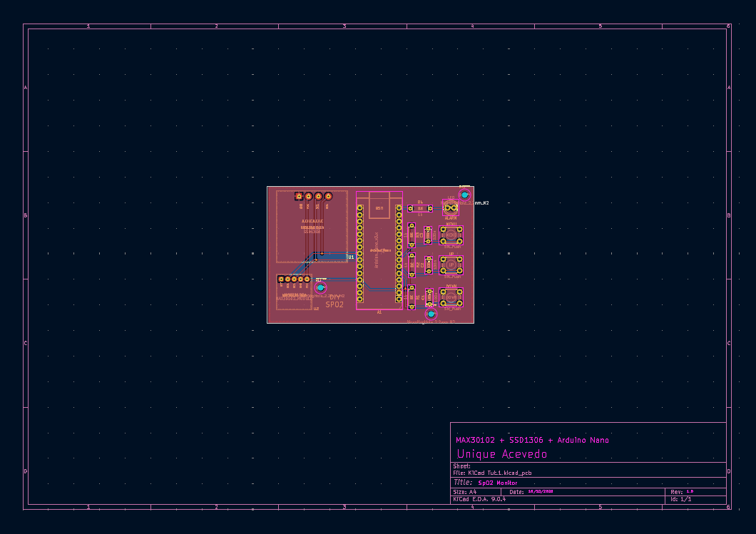
I worked through footprint assignment and a two-layer PCB layout, including the module positions and user controls. The archive includes the editable board and schematic, the project settings, and the module footprint files.
I exported a bill of materials, Gerbers, schematic images, board views, and 3D renders. These files document the design revision; fabrication exports alone do not establish that a board has been built or validated.
02 / Visual record
Open a photo or drawing to inspect the details, or play an available prototype demo.
Vector preview exported from the editable KiCad schematic.
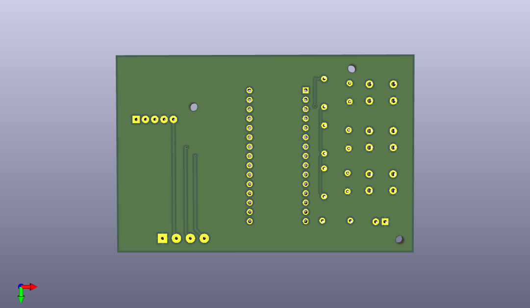
Routing and placement from the board design.
KiCad render of the PCB design; this is not an assembled board.
A second view of the same design revision.
A little time at the workbench
Explore a simple circuit, then step through one of my PCB designs.
My SpO₂ design / 01 of 03
Start with the electrical connections. My SpO₂ schematic links the controller, sensor, display, and controls.
A walkthrough of saved design views, with an animated inspection sweep. These are actual KiCad exports, not a recording of live CAD work.
03 / Bill of materials
Component values and references from the repository BOM. Scroll across for the assigned footprints.
| References | Qty | Part / value | Assigned footprint |
|---|---|---|---|
| A1 | 1 | Arduino_Nano_v3.x | Module:Arduino_Nano |
| C1,C2,C3 | 3 | 100n | Capacitor_THT:C_Disc_D4.7mm_W2.5mm_P5.00mm |
| D1 | 1 | LED | LED_THT:LED_D5.0mm |
| R1,R2,R3,R4 | 4 | 1k | Resistor_THT:R_Axial_DIN0207_L6.3mm_D2.5mm_P7.62mm_Horizontal |
| SW1,SW2,SW3 | 3 | SW_Push | Button_Switch_THT:SW_PUSH_6mm |
| U1 | 1 | SSD1306 | KiCadTut:SSD1306 |
| U2 | 1 | MAX30102 | KiCadTut:MAX30102 Module |
Open the working files
Source files and repository notes are preserved as a project record. Notes may describe intended behavior. See the project stages above for what was built and tested.
What stayed with me
Footprint selection is part of the electrical design, especially when modules are involved.
A schematic, board, BOM, and fabrication package need to describe the same revision.
A 3D view helps communicate placement, but it cannot substitute for assembly and testing.