I built and validated this amplifier in four parts during Electronic Devices Laboratory. Working from the output toward the input helped me understand what each stage needs from the one before it. The circuit explored the functional architecture of the LM741 using discrete transistors.
01
Start at the output
The push-pull Class AB stage drove a speaker load. I observed crossover distortion near the zero crossing and adjusted the bias to reduce it. This made the relationship between transistor operating point and the output waveform much easier to see.
02
Establish the bias
Diode-connected BJTs, current mirrors, and current sources and sinks established the operating points. This stage connected the DC bias calculations to the behavior of the physical circuit.
03
Add voltage gain
I built and integrated a voltage-gain stage, studying common-emitter amplification and Darlington-pair behavior. Frequency-response analysis brought Miller capacitance, bandwidth, and dominant-pole behavior into the design discussion.
04
Close the signal chain
The differential input pair and tail current source completed the amplifier. I examined input symmetry and common-mode behavior while connecting all four stages into one circuit.
02 / Visual record
Look inside the project.
Open a photo or drawing to inspect the details, or play an available prototype demo.
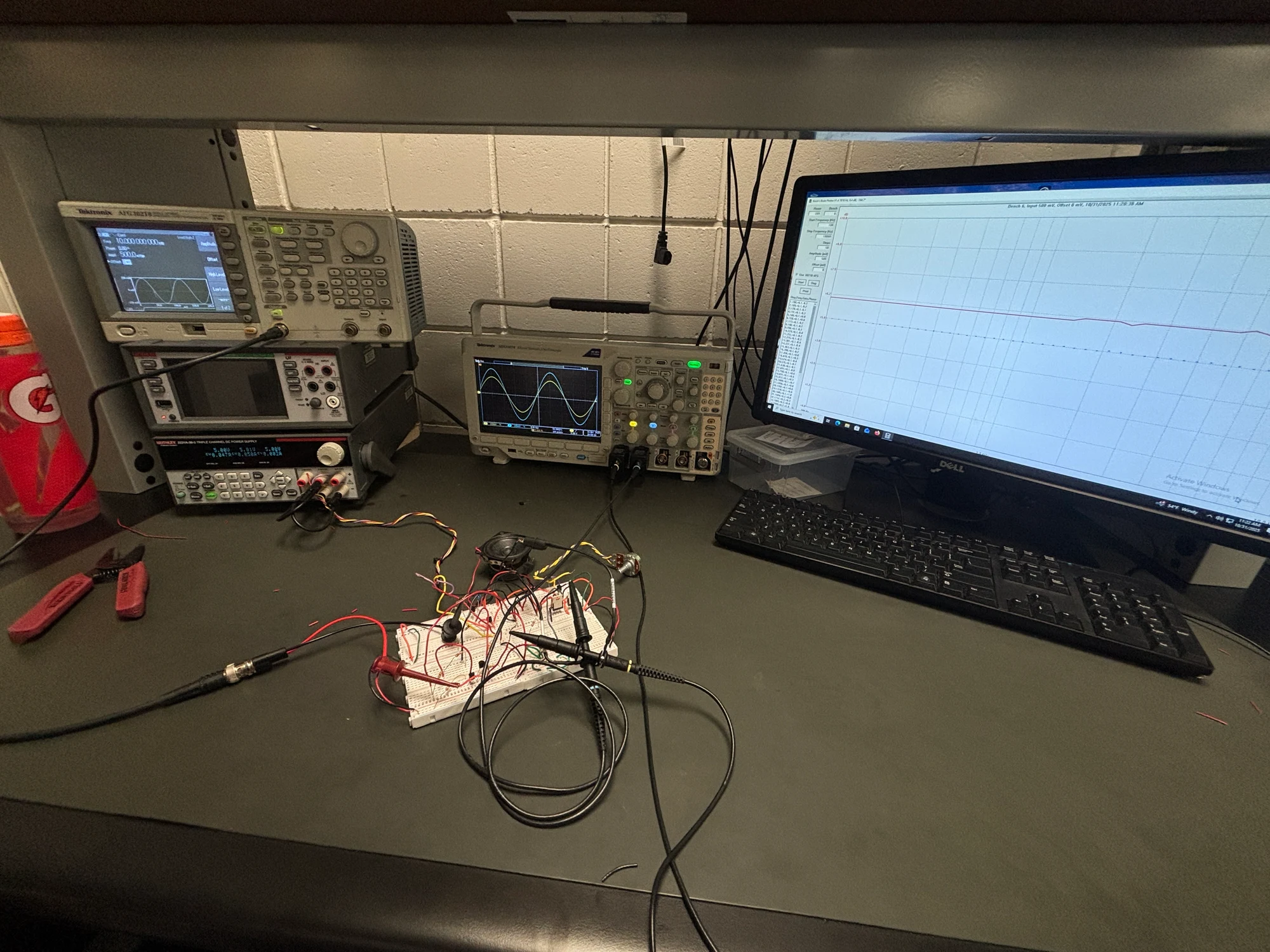
The full lab bench
My breadboard amplifier alongside the function generator, oscilloscope, power supply, and computer display.
Output-stage breadboard
A close view of my breadboard wiring, discrete components, probes, and speaker.
Building the signal chain
Another breadboard configuration from the lab, with transistor circuitry and a potentiometer.
Integrated breadboard circuitry
Connected breadboards with probe points, discrete components, and the speaker used in the lab.
The lab schematic
A photograph of the circuit sheet used during the lab. Component labels and feedback connections can be inspected at full size.
Observing the waveforms
The breadboard setup and two oscilloscope traces during testing. This photograph is a visual record, not a calibrated measurement export.
A little time at the workbench
Connect. Observe. Refine.
Explore a simple circuit, then step through one of my PCB designs.
Calculated current9.1 mACircuit closed
Breadboard learning model
One resistor makes a difference.
Switch the supply or change the series resistor. A larger resistance lowers the current through the LED.
Idealized DC example: I = (5 V − 2 V) / R. The LED has an assumed 2 V forward drop. Animation shows the current path; it is not a measurement or a wiring guide for my op-amp.
Source files and repository notes are preserved as a project record. Notes may describe intended behavior. See the project stages above for what was built and tested.
What stayed with me
Lessons from the work.
A stage can work by itself and still need adjustment when it is connected to the rest of the circuit.
Bias conditions explain a great deal of what appears on an oscilloscope.
Simulation is most useful when I can connect it to a specific bench observation.
Next steps / Still ahead
What I want to document next.
01Add editable circuit files and original measurement records when available.
02Document a repeatable test setup before making numerical performance claims.